Workshop on Hardware for Edge Intelligence
Maximize edge intelligence through fundamental advances linking on-chip edge computing, edge-of-the-node sensing, and in-sensor processing with wireless communication, power budgeting, and integration.
Meeting Agenda
- Feb. 28, 2024
- 2-5 p.m. ET
- Virtually via Zoom
- Attendees: Industry and government technologists, managers, and leaders
Workshop on Hardware for Edge Intelligence hosted by the NSF Industry/University Cooperative Research Center (I/UCRC) on Multi-functional Integrated System Technology (MIST)
2 p.m. Motivation for Center on Hardware for Edge Intelligence by Dr. Toshi Nishida, Director NSF Industry/University Cooperative Research Center on Multi-functional Integrated System Technology (MIST), Professor of Electrical and Computer Engineering, and Associate Dean for Academic Affairs, Herbert Wertheim College of Engineering, University of Florida
2:15 p.m. Invited talk by Dr. Volker Sorger, Director Florida Semiconductor Institute

Future of Edge Intelligence by Dr. Volker J. Sorger
Dr. Volker J. Sorger is the Director of the Florida Semiconductor Institute and the Rhines Endowed Professor for Semiconductor Photonics at the University of Florida. Dr. Sorger oversees and coordinates microchip and semiconductor activities in the state of Florida including R&D and manufacturing private-public partnerships and workforce development programs. For his work, Dr. Sorger received multiple awards including the SPIE Maria Goeppert-Mayer Award, the Presidential PECASE Award, the AFOSR YIP, the Emil Wolf Prize, and the National Academy of Sciences award of the year. Dr. Sorger is an Editor for Optica, Nanophotonics, Applied Physics Rev., eLight, Chips, and was the former editor-in-chief of Nanophotonics. He is a Fellow of The Optical Society (formerly OSA), SPIE, IEEE, IAAM, and The German National Academic Foundation. He holds more than 20 U.S. patents licensed to corporations and ventures.
2:30 p.m. High Level Expertise and Infrastructure supporting Hardware for Edge Intelligence research at University of Florida (UF), University of Central Florida (UCF), and University of Virginia (UVA) by Dr. Toshi Nishida (UF), Dr. Avik Ghosh, Professor of Electrical and Computer Engineering and Professor of Physics (UVA), and Dr. Swami Rajaraman (UCF)
3 p.m. Project Development Process and Level of Interest Feedback Evaluation (LIFE) Evaluation by Mr. Shelby Powell, Managing Director, MIST Center
3:15 p.m. Research Capabilities Proposals
Bio-Inspired Smart Image Sensor for Time-Critical Applications by Dr. Christophe Bobda
Dr. Christophe Bobda is an expert in reconfigurable systems and system-on-chip, hardware/software embedded systems with applications in IoT, cybersecurity, and is-situ image analysis, particularly hardware/software reconfigurable architectures for acceleration of video processing applications, at the edged and in the cloud. Professor Bobda is a Senior Member of the ACM and IEEE. He is also on the program committee of several conferences like DAC, CODES+ISSS, FCCM, FPL, and FPT and was ACM ACM Distinguished Speaker from 2016 to 2020. Dr. Bobda has authored more than 200 journal and conference publications in computer architecture, embedded systems, system-on-chip, embedded imaging, robotics, and cybersecurity. He received multiple conference awards, including the FCCM Best Short Paper and the SBCCI Test of Time Awards.
High-Level Threat Vectors and Risks to Edge Compute Intelligence by Dr. Mike Borowczak
Dr. Mike Borowczak, currently an Associate Professor of Electrical and Computer Engineering at the University of Central Florida, has over two decades of academic and industry experience. He worked in the semiconductor, biomedical informatics, and storage/security sectors in early-stage and mature startups, medical/academic research centers, and large corporate entities before returning to the US public university system full-time in 2018. His current research interests are focused on automation for design, development, and assessment of resilience, robustness, and security of electronic devices and systems which currently includes topics such as: advanced/novel cryptographic logic primitives, assessment and evaluation of assistive technologies on semiconductor design and post-manufacturing operation, development and detection methods for AI-based sabotage. He and his students have published over 100 journal and conference publications. His research has been funded (~$8.5M since 2018) by federal, national, state, and industrial entities.
Devices and Systems for Sensing and Computing in Extreme Environments by Dr. Philip Feng (UF)
Dr. Philip Feng is a Wally Rhines Endowed Professor in ECE and Graduate Faculty in Physics at University of Florida. His research is primarily focused on emerging semiconductor devices and integrated micro/nanoscale systems, especially those in advanced semiconductors (SiC & other WBG), 2D materials and heterostructures, and their heterogeneous integration with mainstream electronic and photonic technologies. Feng received his Ph.D. in EE from Caltech in 2007. He has graduated 13 Ph.D. students and mentored 8 postdoctoral scholars, and supervised 15 M.S. students (with thesis or project), and >20 undergraduates through senior projects, theses, or NSF REU programs (including 2 NSF GRFP recipients). His research and education activities have been recognized by the NAE Grainger Foundation Frontiers of Engineering (FOE) Award, the NSF CAREER Award, the Presidential Early Career Award for Scientists and Engineers (PECASE), and several Best Paper Awards (with his students) at IEEE and other international conferences. He has served for IEEE IEDM/MEMS/Transducers/IFCS technical committees and/or international steering committees, and was a chair for IEEE MEMS 2021. He has been a co-organizer/chair for the annual SiC Materials & Devices Workshop since 2017.
Edge computing in imager towards 3D perception by Dr. Kyusang Lee
Dr. Kyusang Lee is currently an Assistant Professor of Electrical and Computer Engineering and Materials Science and Engineering departments at University of Virginia. He received his B.S. degree from Korea University in 2005, M.S. degree from Johns Hopkins University in 2009, and Ph.D. degree from University of Michigan in 2014, all in Electrical Engineering. He was a postdoctoral fellow in the Department of Electrical Engineering and Computer Science at the University of Michigan, and a postdoctoral associate in the Department of Mechanical Engineering at Massachusetts Institute of Technology (MIT). His research interests highlight the use of thin-film compound semiconductors in optoelectronic devices, with a particular emphasis on applications for imaging and artificial intelligence. He is the recipient of the NSF faculty early career award, AFOSR young investor program award, best student presentation award at the IEEE 38th Photovoltaic Specialist Conference and the UMEI postdoctoral fellowship. His works have been published in Nature, Science, Nature materials, Nature Nanotechnology, Nature electronics, Science Advances, PNAS and Nature communications etc.
Baterryless AI hardware solutions for the Internet of a Trillion Things by Dr. Mircea R. Stan
Dr. Mircea Stan is teaching and doing research in the areas of AI hardware, Processing in Memory, Cyber-Physical Systems, Computational RFID, spintronics, and nanoelectronics. Since 1996 he has been with the ECE Department at UVa, where he is now the Virginia Microelectronics Consortium (VMEC) endowed chair and Director of Computer Engineering. He was a co-author on best paper awards at ASILOMAR19, LASCAS19, SELSE17, ISQED08, GLSVLSI06, ISCA03 and SHAMAN02 and he gave keynotes at iSES23, GLSVLSI23, NILES22, DCAS18, SOCC16, CogArch16, WoNDP15, iNIS15 and CNNA14.
Highly energy efficient RF front end module using metaconductors on fused silica for 3D heterogeneous integration by Dr. YK Yoon (UF)
Dr. Yong-Kyu “YK” Yoon is currently a Professor in the Department of Electrical and Computer Engineering at the University of Florida, Gainesville, FL. His current research interests include three-dimensional (3-D) micromachining and nanofabrication; design and implementation of metamaterial for radio frequency (RF) and microwave applications; micromachined millimeter wave and terahertz antennas and waveguides; bio/microfluidic systems for the lab-on-a-chip applications; wireless telemetry systems for biomedical applications; and ferroelectric material development for high-density memory devices and/or tunable RF devices. He received his BS and MS degrees in electrical engineering from Seoul National University in Korea. He also earned an MSEE degree from the New Jersey Institute of Technology, Newark, NJ in 1999 and a Ph.D. degree in electrical and computer engineering from the Georgia Institute of Technology, Atlanta, GA in 2004. He held a postdoctoral position in the Microelectronics Research Center of Georgia Institute of Technology from 2004 to 2006. In 2006, he joined the faculty of the University at Buffalo, the State University of New York as an Assistant Professor in the Department of Electrical Engineering, where he directed the Multidisciplinary nano and Microsystems (MnM) laboratory until 2010, when he moved to the University of Florida, Gainesville, FL. He received the NSF Early Career Development Award (CAREER) in 2008 and the Young Investigator Award from the University at Buffalo in 2009. He has more than 280 peer-reviewed publications. He is a member of the IEEE society. He actively participates in multiple technical conferences including Microelectromechanical systems (MEMS), Transducers, Hilton Head, micro total analysis systems (µTAS), American Vacuum Society (AVS), International Microwave Symposium (IMS), Electronic Components and Technology Conference (ECTC), and Antenna Propagation Symposium (APS).
4:15 p.m. Feedback and Discussion of Industry Needs
4:40 p.m. Next Steps
5 p.m. Adjourn
About
Connection to MIST Center
Edge Intelligence is a natural progression of the current 3-university (UF, UCF, UVA) MIST IUCRC center. The vision of MIST is “Innovating more than Moore Technology for the IoT era”. MIST has been focused on pre-competitive research on the development of the general hardware infrastructure for the IoT in the post-Moore’s law era since 2014. IoT has created a large commodity market for wi-fi connected appliances, infrastructure, consumer goods, vehicles, wearables. Currently 50 billion IoT devices are connected to the internet, projected to be 80 billion by 2025, with 2000 zettabytes of data generation expected by 2035. However, a large volume of these connected systems are deployed nowadays near the end user. With the growth of mobile computing and the AIoT (Artificial IoT), a natural progression of our center goals follows a global trend of pushing processing to the edge right where data is being generated. For many applications such as mine robots, autonomous vehicular transport or Mars Rovers, reliance on a wi-fi connection or accessing a cloud is risky (e.g. in enemy territory), unfeasible (underground, underwater, on remote terrain, on another planet) or undesirable due to costly upload-download and communication delays. The need for manageable cost, latency, reliability, scalability, diversity and privacy makes Edge intelligence an inevitability.
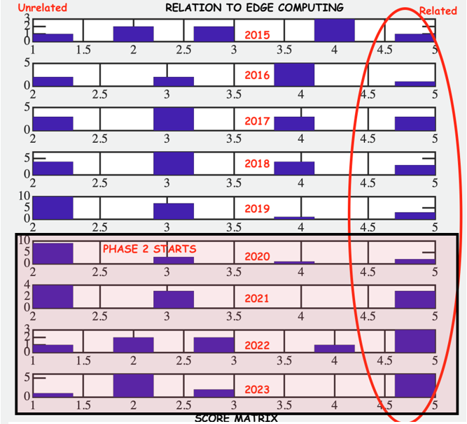
MIST center projects have naturally gravitated over the years toward Edge Intelligence, as captured in the yearly histogram plot to the right. All projects were ranked by experts on a scale of 1 to 5 (5 meaning directly relevant to Edge Intelligence, 1 unrelated). There is a clear natural migration in the plot, especially since the start of Phase-2, along with accompanying publications, proposals and IP generation in that space.
A notable accomplishment in this direction is an invited blog by SEMI that faculty from all three sites participated in, titled “Maximizing Edge Intelligence requires more than computing.”
Economic relevance of the research area of the Center
According to Gartner, the top two trends shaping the future of data science and machine learning includes Edge AI. The US semiconductor industry is teaming up with DARPA and NSF to invest in multiple initiatives for university research in areas including RF to THz sensing, cognitive and distributed computing, intelligent memory and storage, advanced devices and architectures. The proposed Edge Intelligence center can act as a sandbox for many of these topics.


Thrusts
- Edge Computing
- Edge Sensing
- Edge Wireless
- Edge Power
- Edge Integration
Research Goals
The current MIST center spans five research vectors – computation, wireless, power, sensing and integration. In each thrust area, there are new emerging challenges at the edge, as summarized in our invited SEMI blog that the sites co-authored. Edge intelligence will extend these vectors right to the physical world for instant and accurate data sensing and processing, for intelligent decision-making. This requires tailored algorithms for real-time ML/AI, simultaneously being resilient to sub-optimal power, erratic wifi and harsh environments. The Edge Intelligence goal is to revisit the fundamental duo of on-chip mist computing (pushed to the edge relative to cloud and fog computing), and edge-of-the-node sensing, along with wireless communication, power budgeting, and integration, to maximize utilization of edge intelligence.
The MIST leadership and their IAB went through a strategic roadmapping exercise. The AirTable Survey established a goal of identifying specific research thrusts of interest to our IAB member companies (and will continue to serve as a survey for future members). The survey asked the IAB to rank their preference on a 1-5 score on various subtopics within (a) Computing at the Edge, (b) Sensing at the Edge, (c) Power at the Edge, (d) Wireless at the Edge and (e) Integration at the Edge. The result is shown below:
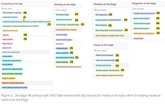
Accordingly, our proposed research thrusts within each subarea are:
- Edge Computing: Neuromorphic Computing, Compute-in-memory, Federated edge learning (edge computing + ML), Edge Analytics, and Edge AI.
- Edge Sensing: Biological Edge, Harsh environment, Multi-modalities, Novel materials, On the body wearable edge, Optoelectronics and Reconfigurable sensing.
- Edge Wireless: 5G Integration, EMI Shielding, Low power communication and Reconfigurable communication
- Edge Power: Battery tech, Energy harvesting, Wireless power transmission and Ultra low power design.
- Edge Integration: Flexible hybrid integration, Heterogeneous integration, Hybrid technologies, Multi-chip modules and SWaP optimization.
Edge Computing: low-power processing and reconfigurable memory
Deep learning and AIoT at the edge is fundamentally constrained by energy, requiring ~1 Terabit of operation per second at ~1 milliwatt of power. This will require across-the-stack innovation. For instance, most deep neural nets suffer from ‘stability-plasticity’ dilemma – accommodating new data without data overwrite, exacerbated if we need this to be executed fully on-chip with limited memory and energy budgets. This may necessitate adopting algorithms executed in the brain, such as adaptive synaptogenesis, as well as novel material platforms such as low-barrier magnets that can couple wirelessly and are programmable as probabilistic bits with very low footprint. Similarly, CMOS oscillators based on mature, time-tested technology could trade memory for accuracy and be scaled for large circuits.
Edge Power: strategic vs opportunistic energy harvesting
Along with energy-efficient hardware, the projected Internet of a Trillion Things (IoTT) will need diverse power sources including batteries augmented with energy harvesting solar, thermal or RF sources. Energy harvesting will vary from the opportunistic hunter-gatherer strategy (scavenging indiscriminately – cheap but unreliable) to deterministic industrial agriculture strategy such as wireless power transmission inspired by RFIDs.
Edge Sensing: harsh environments and saliency detection
While commercial sensors are prolific for consumer IoT, many edge applications need to deal with harsh environmental conditions such as extreme temperature, pressure, liquids and radiations – for applications such as Mars rovers, aerospace, industrial turbines, bio-chemical reactors, which will require appropriate materials, transducers and packaging for harsh sensing technologies. At the same time, real-time processing schemes can mimic the retina by looking for salient events on-chip in event cameras and artificial eyes.
Edge Integration: IC and system Integration
The former will require dense 3-D heterogeneous, frequently back-end-of-the-line integration of diverse material stacks, with high alignment accuracy on silicon chiplets, dense vias for compact non-volatile memory, SoC for monolithic and heterogeneous integration of beyond-CMOS devices, RF/analog components and rad-hard spintronics, not to mention wide band on-chip. Techniques such as remote epitaxy and hybrid bonding can prove critical to these efforts.
Edge Wireless: metaconductors, metamaterials, and novel actuation
Wireless at the edge would require dealing with lossy interconnects, or miniature on-chip antennas that can bypass the EM limit. Metaconductors can use multiple magnetic and non-magnetic layers to reduce RF resistance and power consumption, while meta-materials can reduce their sizes further by energy-efficient actuation of lattice and spin waves and engineered nonlinearity that alter the operating frequency to resonant rather than EM frequency. Particle-like excitations in antiferromagnets can push these to very high (~THz) resonant frequencies and drive them with current at well over 100s of meters/second speed. These mechanisms can allow much smaller sizes, higher frequency compatible with 5G/6G, as well as low-frequency lossy communication (e.g. underwater, implants).
Register Now
This meeting is free and open to the public. Registration is required.